Developing demands and the market show two main trends helping to shape the ongoing development of system integration technologies. First of all is an ongoing increase in the number of functions directly included in a system — such as electrical, optical, mechanical, biological and chemical processes — combined with the demand for higher reliability and longer system lifetime. Second is the increasingly seamless merging of products and electronics, which necessitates adapting electronics to predefined materials, forms and application environments.
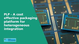
Large area mold embedding technologies and embedding of active components into printed circuit boards (Chip-in-Polymer) are two major packaging trends in this area. Both technologies are under the frame of Panel Level Packaging research at Fraunhofer IZM.
 Fraunhofer Institute for Reliability and Microintegration IZM
