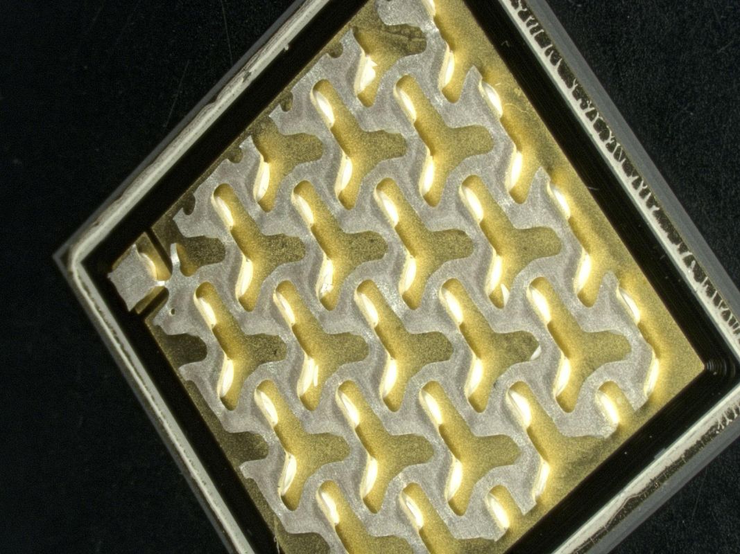
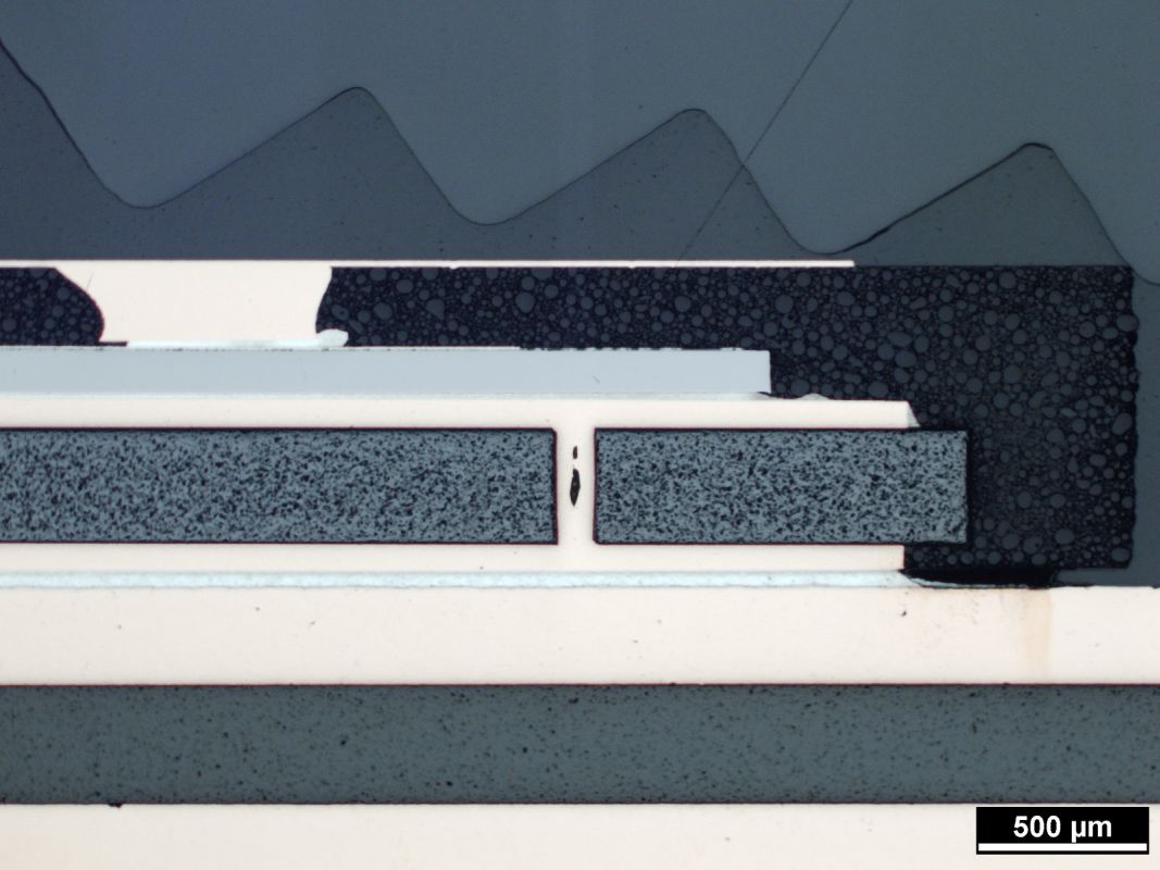
Fraunhofer IZM introduces a package alternative to commercially available PCB-based Power CSPs: a mold-embedded power die, addressing power electronics packages requirements as good thermal conduction to bottom and also to top; high thermal mass on top for Wide Band Gap short circuit capability and low production cost. Major difference to PCB-based single chip packages is the use of an isotropic isolating material. Furthermore, the top-side interconnects were realized by bulk material instead of common filled Cu vias, enabling the thermal path on top side and also avoiding risky laser drilling process for interconnection between top die pads and top package pads. Prototypes were developed with 1.2 kV Si MOSFETs; layout adaptions to alternative die types is possible.
Technical innovation is the application of Compression Molding process for encapsulation of assembled power dies, allowing a high volume encapsulation up to 18”x24” mold tool size. The following technical aspects have been investigated:
- Possible damage of die during assembly and encapsulation → >90% yield for first prototyping
- Interface & package integrity → active power cycling: >180.000 TC passed // H3TRB: 4 of 6 passed // MSL1 passed
- Warpage after encapsulation → mimized warpage by suitable material selection
- Metallization of molded surface → enabling topside interconnection either by soldering or sintering
 Fraunhofer Institute for Reliability and Microintegration IZM

