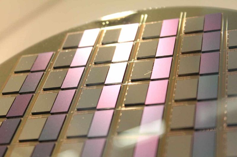
High-End Performance Packaging – A New Paradigm for Electronics Integration
Chiplets


Advanced packaging technologies like flip-chip integration, wafer-level CSPs, or ICs embedded in the substrate play a crucial role in modern electronics manufacturing. As demand for faster and more efficient computers and other electronic devices continues to surge, innovative packaging solutions are becoming increasingly sought after.
Industry and research have responded to the market’s call with new techniques and novel architectures like chiplet designs or heterogeneous integration, all of which promise more powerful systems at lower costs.
A related trend sees the move away from passive system carriers (i.e. interposers or high-end substrates) to system designs that give the carriers an active role in supplying some of the functionality of the system.
The advent of chiplet architectures has paved the way for this and continues to influence the direction of travel. Chiplets are tiny chip units that can work monolithically or be combined to provide the systems’ functions, contributing with unique flexibility to the idea of a system-on-chip.
Each chiplet is designed to have a separate and independent function and to be combined with other chiplets for a custom solution for each given application.
The concept is extremely flexible and scalable – in the system’s design and its production – and reduces both the time-to-market and the cost of developing innovative products.
The advantages of the chiplet architecture are evident: By breaking down the old, monolithic single-chip design into smaller, more versatile components, designers can enjoy the benefits of established, tested technologies while working on novel, innovative components. This makes the design process faster and leaner, makes success with the “first silicon” more likely, and reduces production costs with better utilization and better yields with the 300 mm wafer substrates.
Fraunhofer IZM was quick to realize the potential of these trends and to pursue the idea of a top-down “disaggregated system”, banking on the Institute’s extensive knowhow in advanced packaging.
The Institute recognized the need for processing standards that would be accepted in the industry and became the first organization in Europe to forego specific R&D processes in favor of hybrid bonding combined with through silicon vias (TSVs), which has now been established as the standard approach across the industry.
Fraunhofer IZM has been behind many of the advances in micro-bumping for flip-chip integration with extremely dense contacts, as are now used in chip stacking. This has been part of the Institute’s innovation strategy for a full three decades, making this packaging toolbox the natural choice when testing the chiplet paradigm, which already arranges the front-end architecture in separate, IP-centric hardware units, for high-performance systems.
A trend towards heterogeneous integration is accompanying this new architectural paradigm from the digital domain.
Using the chiplet architecture adds substantially to the technological options, including the ability to integrate several technologies, like logic controllers, memory, analogue functions, or sensors, to a single chip-sized (sub) system. The end product is a highly versatile module with greater performance and better energy efficiency.
Even further up the value chain in packaging, innovative approaches are complementing the concept of High-End Performance Packaging (HEPP).
This HEPP approach to electronics integration is being powered by the availability of substrateless fan-out packaging, which allows extreme circuit and contact densities at large panel sizes, with active interposers and functional properties inherent to the geometry (e.g. directional antennas, integrated cooling). It charts a clear path towards meaningful heterointegration.
 Fraunhofer Institute for Reliability and Microintegration IZM

