Fraunhofer IZM - Archive

You love hearing about the latest research in microelectronics, but the technobabble just confuses you?
Don't let accronyms, abbreviations, and specialist terminology limit your curiosity.
Our archive collects all of the terms and definitions from the everyday work of a leading research institute and helps you navigate them with clear and easy-to-remember explanations.
Our little µ is just as interested and committed as you and will add a new term every month.
And if you do get stuck, send us an email, and we will ask our Fraunhofer IZM specialists to help you out.

Where to start: Just start scrolling and learn more about panels, cleanrooms, ICs and much, much more.


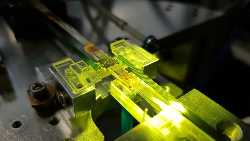
Photonic integrated circuit (PIC)

A photonic integrated circuit (PIC) contains multiple photonic components, such as waveguides, modulators, and detectors on a single chip to manipulate and transmit light signals. Similar to electronic integrated circuits (IC), PICs aim to miniaturize and enhance the performance of optical systems by reducing size, cost, and energy consumption.

Tech News - Photonic Kit for Network Architecture at Speeds above 50 Terabits per Second  

Photonic integrated circuit (PIC)
© Fraunhofer IZM

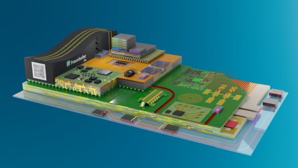
System integration

In system integration, individual discrete units or components are combined on a substrate. This results in integrated circuits (ICs) that can perform more complex tasks, such as computer chips. Successful system integration therefore ensures that the various components work together correctly as part of a single system. As the number of components in a circuit increases, so does the level of integration and therefore the potential performance of the system.

© Fraunhofer IZM | Volker Mai

D-Band

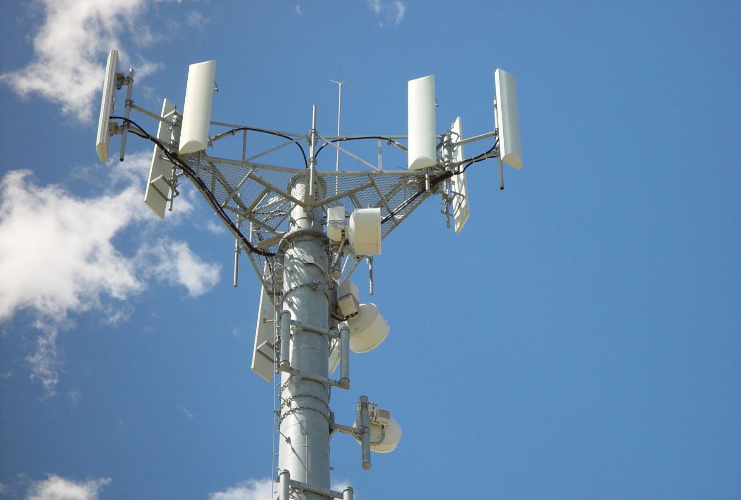
The so-called D-band is a microwave frequency band that describes the range of radio frequencies from 110 gigahertz to 170 gigahertz in the electromagnetic spectrum. Signals in this range have a very short wavelength in the single-digit millimeter range. As the D-band frequency range offers a higher bandwidth than other microwave bands, it is a potential candidate for the next generation of 5G and 6G mobile communications as well as for future radar applications.

Communication Module Development


Antennenmast - Mikrowellenfrequenzband
© Fraunhofer IZM

Microchip

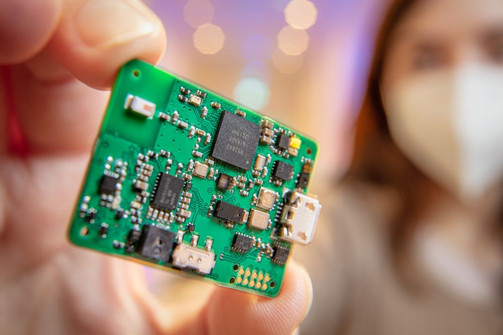
A microchip - also known as an integrated circuit (IC) - is a small electronic component. Microchips are manufactured on a semiconductor plate and serve as the core building blocks of modern electronics. Microchips contain transistors, capacitors and resistors that are arranged and integrated on a thin substrate to perform a variety of functions. Microchips are used when it comes to computing power, data storage, signal processing and communication. Typical applications include computers, smartphones, household appliances, automotive electronics and medical devices.

Using magnetic effects in electrons for a hundredfold reduction in the power consumption of future chips

Mikrochip
© Fraunhofer IZM | Volker Mai

Glob top

A glob top is a type of encapsulation used in microelectronics to protect exposed components from dust, moisture, solvents and dirt. The encapsulation can be solid or flexible and is cured under UV light, visible light or thermally. A glob top can also protect integrated circuits, wire connections and chip-on-board applications or be used to attach circuits to glass or PCBs. Special plastics are used for this purpose, which are produced in different viscosities for the various applications.


Glob Top
© Fraunhofer IZM

Superconductors

When electricity is transported, losses are normally expected, for example in the form of heat. Superconductors are used to avoid these losses: These are materials that no longer exhibit any electrical resistance at very low temperatures close to absolute zero. Another property of superconductors is the so-called Meissner-Ochsenfeld effect, in which magnetic fields are completely displaced from the interior of the material. Due to their high current-carrying capacity, superconductors are particularly in demand in the field of energy technology.

Quantum Computing/ HalQ


Schwarz-weiß Mikroskop Aufnahme - Fine-Pitch-Kontakte
© Fraunhofer IZM

Energy label

This label provides information about the energy consumption and efficiency of a product. They ensure greater transparency and are intended to help consumers make informed purchasing decisions. Large electronic appliances such as washing machines and fridges have already been categorized into energy efficiency classes by the labels for years. In the future, energy labels will also be extended to other product groups such as smartphones and tablets.

Sustainable mobile devices for the environment: Long live smartphones and tablets! (REALIZM Blog)

Working Group - Policy, Ecodesign and Circular Materials (PEC)


Low-power Electronics

Low-power electronics are characterised by special energy efficiency and long battery life. For example, sleeping sensors or energy harvesting technologies are used to minimise energy consumption. Low-power electronics are used primarily in wearable devices such as smartwatches, but also in the smallest medical technology such as pacemakers or robust IoT devices, which are operated long-term without an external power source.

Towards Zero Power Electronics (youtube)


Biene - Bee
© Fraunhofer IZM | Volker Mai

Quantum photonics

Quantum photonics deals with the interaction of light particles and quantum mechanical systems. Various methods are used to investigate and control phenomena such as entanglement and quantum states of photons. Fields of application are, for example, the secure transmission of information via quantum communication and quantum computing. Researchers continue to work on developing new technologies to enable higher performance and security in data processing and transmission with the help of the laws of quantum mechanics.

Working Groups - Optical Interconnection Technology

The glass revolution of quantum systems (REALIZM)

Thermal Management

Keeping powerful, miniaturized electronics working reliably and for long means finding a way to channel away the heat created during operation. The answer is thermal management: Flaws and weak spots are identified and designs optimized by characterizing and simulating the materials, packages, and entire systems with due consideration for the many factors influencing the equation.

Services - Thermal Management

µ fragt nach: Komplexe Begriffe – einfach erklärt
© Fraunhofer IZM

Optical Fibers

Optical fibers transport masses of data around the world every day. The data passes through the fibers in the form of light signals: Optical fibers are a form of light waveguides. Fraunhofer IZM is also researching everything from new types of optical fibers like hollow-core fibers to the coupling and integration of these fibers.

Fiber Lensing

Heterogeneity

As with software, hardware can also be called heterogeneous if different packaging techniques are used in a single system. How each element operates is strongly influenced by the other elements. Microsystems are one example of this, which combine sensors, the means for data processing, power supplies and wireless communication in a single component.

Wafer Level System Integration

Chiplets

Wafer
© Fraunhofer IZM | Volker Mai

Chiplets

Chiplets are the individual building blocks of a chip. Instead of a complete, monolithic silicon chip, modular units can be combined to form larger ICs, allowing more flexible designs. They are less susceptible to processing defects and can increase performance on limited space. Chiplets can also be replaced and recycled, which makes it easier for systems to be updated and refreshed.

Feature Topics Chiplets

image - 3D-Modul mit TSV-Interposer und mittels FlipChip-aufgebauten Elektronikkomponenten als Vorstufe für die Chiplet-Technologie
© Fraunhofer IZM I Volker Mai

Through-Glass-Vias

With its excellent dielectrical properties, glass is a perfect substrate for RF and photonics applications, but it needs ducts through the glass to route electrical signals and make glass suitable for 3D integration. This is done by metallizing ultrafine holes in the glass - called Through-Glass-Vias. These TGVs are formed by laser driling and/or etching through the material.

TGV-Integration

Galvanic

Electroplating, AKA galvanic deposition, refers to the deposition of metal layers on the surfaces of certain substrates by the power of electricity. It works by connecting a DC current through an electrolytic bath. Substrates in that bath receive a uniform metal layer or existing layers are changed in the process. Electroplating can open up new applications for packaging and sensor technology.

Micro Galvanics

Corrosion

For material scientists, corrosion refers to a systemic property that describes how a metal material reacts to its environment. This chemical or electrochemical reaction can change the material and its functional properties. One common example is how iron or steel rust when exposed to water and oxygen. In microelectronics, there are special ways of encapsulating components to avoid such degradation and ensure that systems last for the longest possible time even under adverse conditions.

Corrosion, Electrochemical Migration and Humidity Diffusion

Corrosion-resistant sintering technology for applications at risk of corrosion

Corrosion Analysis Lab


Sensor nodes

Sensor nodes are computers of varying size that can communicate wirelessly with other computers. Together, they form complete sensor networks in which their role is to collect environmental data (e.g. changes in temperature) and pass it on for processing further down the line.   

Research News - Economical wireless communication

Sensorknoten - µ fragt nach: Komplexe Begriffe – einfach erklärt
© Fraunhofer IZM | Volker Mai

Transducer

The term "transducer" refers to all electronic systems or components that transform energy from one form to another or turn one physical quantity (e.g. voltage) into another (e.g. frequency). We can distinguish between transducers that convert forms of energy, transducers that transform information, or inverters that convert alternating to direct currents.

Compact converters enabling high power density

MEMS

MEMS (Microelectromechanical systems) are tiny components that pack electronic switches and micromechanical structures on a single chip to process electrical and mechanical signals. They are the indispensable building block for innovative microelectronics. Their miniature size, low-cost production, and thrifty use of enery makes MEMS particularly appealing for applications like high-frequency systems.

Hermetic MEMS & Sensor Packaging

Flip-Chip

Flip chip is a technology used in semiconductor packaging and interconnection. It works by connecting carrier-less semiconductor chips not by wires, but by solder bumps. These chips are flipped and mounted on the substrate with their active side downwards. By contrast to conventional wire bonding, this means that the entire surface of the chip can be used, shortening the connections and improving performance.

Flip Chip Adhesive Bond Technologies

Condition monitoring

For electronic systems to be as long-lived and sustainable as they can be, their reliability and efficiency need to be understood. Data is collected in the field and interpreted to draw meaningful conclusions about the current state and likely remaining lifespan of the systems. These insights are particularly helpful for preempting and avoiding complete failures with targeted maintenance and for understanding the mechanisms behind such failures by analying the damage that caused them.

Key Research Areas - Condition monitoring of electronics

Key Research Areas - Methods of system evaluation

Project AMWind - Condition monitoring for wind turbines

Thermoforming

Thermoforming uses heat, pressurized air, and vacuums to shape thermoplastic materials like polycarbonates or polyurethane, for example to give electronics components a three-dimensional shape. Switches, LEDs, sensors, and other functional parts must not be damaged in this process, which is why they need to be elastic and laid out in waves or meandering designs

Key Research Area - Thermoforming

TSVs

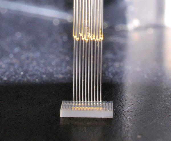
Through-Silicon Vias (TSVs) are electrical connections used in semiconductor design to connect individual chips in 3D-integrated circuits. The metal connections allow smaller, but more powerful designs that are employed e.g. for tamper-proof cryptographic chips or AI-based medical analytics systems. 

TSV-Integration

TSV - Through-Silicon Vias (dt.: Silizium-Durchkontaktierungen)
© Fraunhofer IZM

Interposers

Interposers are routing carriers that make it possible to get different designs aligned and working together in a microelectronic system. With these electronic interfaces, even completely unrelated components can be connected. Interposers can be made from silicon or other circuit board materials and even from glass.

2.5 D Interposer

Interposer Module

Cu-TSV Interposer

Image Interposer - Modul
© Fraunhofer IZM

Sputtern

In sputtering, solid materials are bombarded with highly charged ions, causing atoms to be ejected and enter the gas state. In microelectronics, conductive, semiconductive, and insulating layers are usually formed on the wafer level. Sputtering is used to clean or deposit a coating on surfaces or as an analytical means to understand a surface's composition.

TGV-Integration

Coating system

Sputtern
© Fraunhofer IZM

M3

Methods, Models, Measures (M3) captures the working principles of the Fraunhofer IZM "RF & Smart Sensor Systems" department. It covers the three steps that put electromagnetic field and network theories into practice: Methods are developed to feed into models, based on which actual measures can be taken to create cost-efficient high-frequency components, modules, and systems. The M3 approach is also a perfect choice for optimizing the electromagnetic reliability of individual components.

Working Group - Radar Frontends & Modules

Best Paper of Session Award for SATCOM Research


© vegefox.com - stock.adobe.com

Polymer

Chemically speaking, a polymer is a compound that consists of branched, so-called macro-molecules. The term polymer itself means "made from many similar parts". The plastics that are popular in microelectronics due to their reliability and low price point are usually synthetic polymers. They are used for creating structures with polymer photoresists, for optical waveguides, for 3D printing, or for underfilling and encapsulating chips.

Polymer assembly and structuring technologies for optical and fluidic applications

Radar

The term radar is the abbreviation for "radio detection and ranging" and includes various detection and locating methods and devices based on electromagnetic waves in the radio frequency range. Radar was primarily designed for military purposes, but is also becoming increasingly popular in the development of autonomous driving.

KoRRund - 360° real-time capture: Using 3D radar sensors to drive autonomously without blind spots

Cost-effective packaging for radar sensors


teaser- PM-KoRRUND
© Fraunhofer IZM

Substrate

A substrate, in simple terms, is something that sits underneath something else, i.e. a material basis that can be processed to have different properties. In electronics, the term usually means a circuit board. When chips are made, the wafer that is used as their basic material is also called the  substrate. Usually, the surface of the substrate would be coated and refined for smoother processing.

Embedding & Substrate Technologies

Substrate Integration Line

Substrate Finish and Reliability

Panel

The term "panel" goes back to the French "panneau" (meaning a flat board). In consumer electronics, it typically refers to a user interface, like the touchscreen of a smartphone or a computer. However, in the development and manufacturing of electronics, it  means the full-format substrate for circuit boards, optimized for mass production. A standard panel measures 610 by 457 mm or 24 by 18 inches.

Panel Level Packaging Consortium

Panel Level Packaging

Tech News – Panel Level Packaging is on the way to the next level: PLC 2.0

Eco-Design

The philosophy of designing products in a way that is least harmful to the environment. Eco-design concerns not just the manufacturing of the products, but their entire lifecycle (through their use and to their end-of-life). Environmentally sustainable product design uses special analytical methods to understand the product’s eco balance (including its carbon footprint) and other aspects, such as the ability to repair the product.

Environmental assessment for electronic systems

Learning Factory for Ecodesign

© Fraunhofer IZM

R&D

Acronym for Research & Development.  Scientific methods are used to generate new applicable and practice-oriented insights. The work is financed by investments from industry and public funding. This is how Fraunhofer IZM funds its work.


Smart Textiles

If textiles are combined with electronics, the functionality of the textiles is expanded: they then react to environmental influences with changes in properties. It is possible to weave in electrically conductive fibres, embroider them or print electronics on the textiles. This is particularly useful for measuring vital functions of patients or athletes and indicating changes.

Key Research Areas - Smart Textiles

Key Research Areas - Textile Circuit Boards

Tech News - High-Tech Fashion – art and science for the clothes of tomorrow

Image - Smart Textiles - Archiv
© Fraunhofer IZM

Embedding

To further minimise electronic systems, attempts are made to stack individual components 3-dimensionally. This can be done, for example, by embedding integrated circuits (ICs) directly into the circuit board. In this process, the electronic components are already integrated into one or even several assembly layers and connected to each other during the production of the printed circuit board. This results in highly compact electronic systems - in printed circuit boards, textiles or wafers.

Process and Product Development - Embedding

Key Research Areas - Embedding PCB Technologies for Power Electronics

Key Research Areas - PCB Embedding

Embedding - mue fragt nach / mue knows best
© Fraunhofer IZM | Volker Mai

Printed circuit board

One could call the printed circuit boards the workbenches of electrical engineering, because they are present in almost all devices. They are the carriers of all electronic components and connect them electrically and mechanically. The so-called surface mount technology (SMT) is usually used to assemble the components. The circuit board design is crucial for the later correct functioning of the system, because especially in high-frequency technology the distances between conductor tracks have to be kept exactly, e.g. to prevent crosstalk of signals.

Embedding PCB Technologies for Power Electronics

PCB Embedding

Textile Circuit Boards

Electro-optical Circuit Board

Leiterplatte
© Fraunhofer IZM | Volker Mai

Wirebonding

Thin wires that connect integrated circuits with other electronic connectors or casing. The bonding wire is usually made from gold, aluminium, or copper at a minimum diameter of 12.5 µm, although it can be substantially larger to handle the required electrical currents, especially in power electronics. The wires are connected to components with a specialized micro-welding technique: wirebonding. Wirebonding and soldering are the two standard processes for electrical bonding in semiconductor technology.

Process and Product Development -  Wirebonding

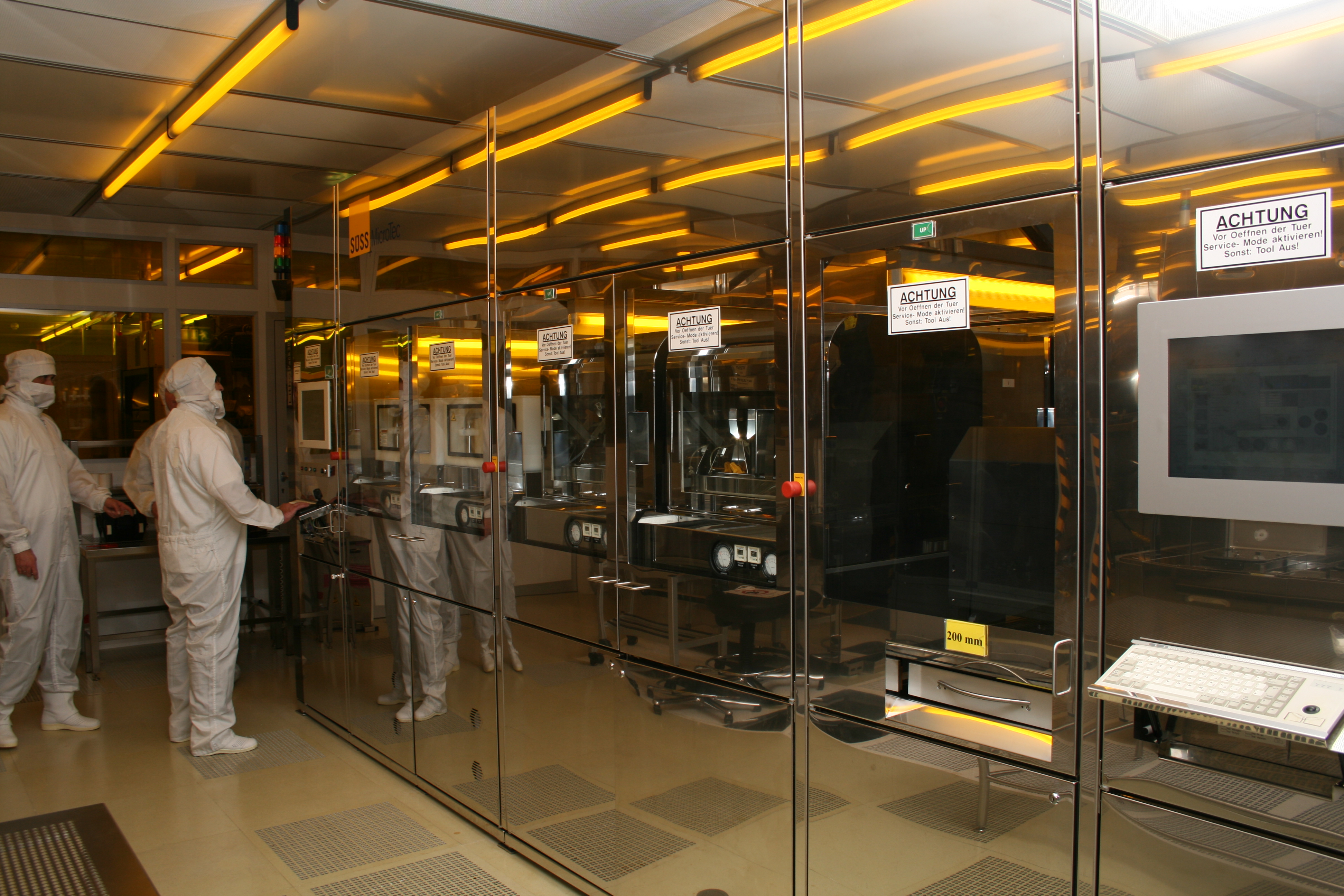
Clean rooms

These are rooms in which the concentration of airborne particles is artificially kept to a minimum. Temperature and humidity – all parameters must be adjusted to enable the highly complex production conditions. 7 nm technologies are currently being introduced in semiconductor production. A hair has a diameter of about 10 µm, which corresponds to 10,000 nm. Clean room classes are differentiated according to the number of particles per cubic meter of air.

What Fraunhofer IZM does in its clean rooms.

6G

The sixth generation of mobile communication, planned to succeed the new 5G standard in ten years or more. 6G intends to increase transmission rates and decrease latency substantially and will employ a higher frequency range. The expected frequency of over 100GHz will create higher free space losses, requiring even shorter distances between transmitters and receivers than with current standards.

Fraunhofer IZM Branch Lab for High Frequency Sensor Systems in Cottbus

Fraunhofer IZM | Volker Mai
© Fraunhofer IZM | Volker Mai

IC

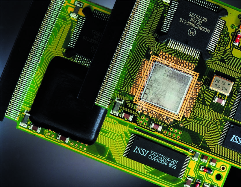
Integrated Circuits (ICs) are electronic circuits that are mostly based on transistors. Since these are manufactured together on a silicon wafer, they are also called monolithic circuits ("made of one stone"). With today's smallest semiconductor technology (14 nm nodes), several billion transistors can be manufactured together on one IC. For protection and contacting, they must be encapsulated in chip packages - this is called electronic packaging.

Tech News - Fraunhofer IZM is joining the EUROPRACTICE IC Service platform

Key Research Areas - Advanced IC-Design

Technical Article - IoT Systemsfor SMEs (Download PDF)

Was sind ICs? Integrierte Schaltkreise (IC) sind elektronische Schaltungen, die zumeist auf Transistoren basieren.
© Fraunhofer IZM

Obsolescence

Obsolescence means the wear and aging of products caused by their construction or materials. There are two types of obsolescence: Absolute obsolescence is determined by a product's technically feasible lifespan. Relative obsolescence refers to the end of a product's actual time in use and can be influenced by technological innovations, new fashions, or commercial considerations. Fraunhofer IZM is investigating the scale of the issue in the German government's largest obsolescence project to date.

Tech News: Fraunhofer IZM leitet EU-Projekt zu vorzeitiger Obsoleszenz

© Fraunhofer IZM | Volker Mai

Sensor

Sensors are used to record physical or chemical quantities. The recorded analogue data is converted into scaled (digital) electrical signals and can then be evaluated. There is an enormous range of sensors, some of which are based on the human senses, but also cover areas that humans cannot detect, such as radar, pH value or even radiation in the non-visible range.

Radar sensor module to bring added safety to autonomous driving

Tracking down polluters

Sensor Development and Integration

Sensor Nodes & Embedded Microsystems

Hermetic MEMS & Sensor Packaging

RF & Smart Sensor Systems

© Fraunhofer IZM

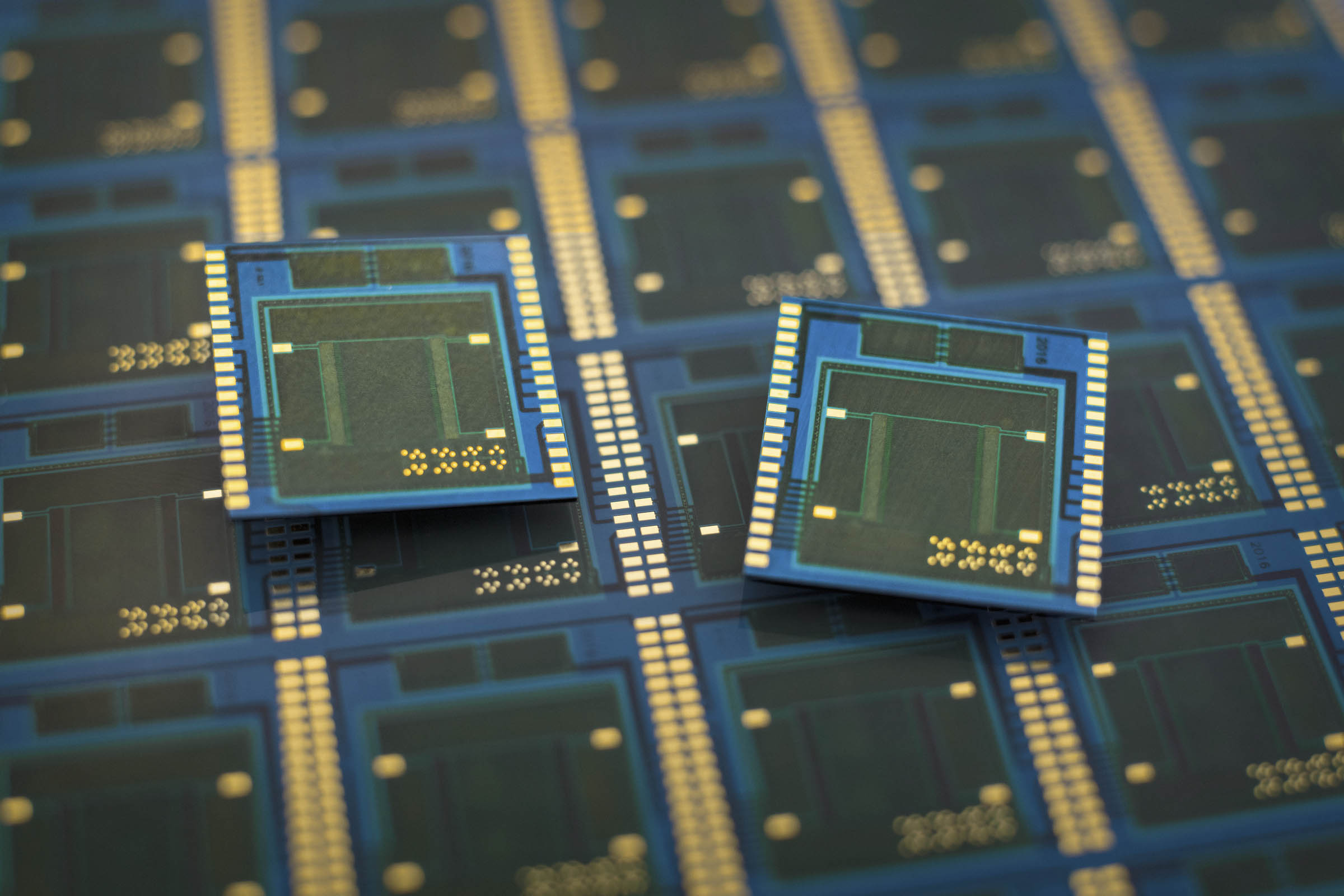
Wafer

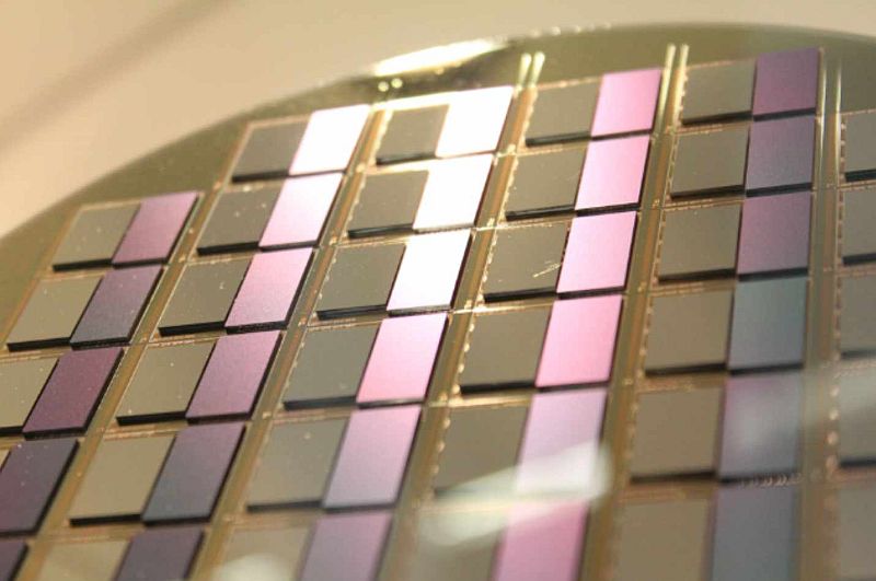
In electronics, the term wafer is usually understood to mean silicon substrates (Si): round substrates, based on single crystals in microelectronics and square, polycrystalline in solar technology. Due to their semiconducting properties, the wafers can be used to manufacture transistors using special doping processes. As a pure substrate material, on which electrotechnical components are wired together, there are also wafers made of glass, ceramics, metal and plastic.

What you can do with wafers

Good to know